Die shots of Commodore chips
Content
IntroductionVIC2 / MOS 6569 R1
VIC2 / MOS 6569 R3
SID / MOS 6581 R2
SID / MOS 6581 R3
SID / MOS 6581 R4
SID / MOS 8580 R5
REU Controller / MOS 8726 R1
more sources
Introduction
In May 2008 I had been graduating in surface science (physics) and had access to some instruments. Also some kind people sent me chips where I could test what method works best to make useful die shots. After a short investigation under a light microscope it turned out that it would be sufficient enough to map the die with the large structures sizes. Any method with higher resolution would just increase the preparation efforts tremendeously and it would have a too high resolution to finish a mapping of the die in a reasonable time.I looked a bit around and the optics group had a very suitable instrument. The microscope is an Axioplan 2 from Zeiss with a software driveable XY-table with micrometer precision and a CCD camera. All mapping images were taken with impinging light. A few parts were looked at in Darkfield mode. Darkfield mode means that the lightsource is at an small angle and the microscope optics sees only the diffuse refracted light. So there can be seen edges more pronounced.
Some credits first:
- support from the optics group, especially Moritz Beleites- VIC2 dies from Stephan Lesch (ceramic R1 and R3)
- SID 6581 R3 die from Tommi Lempinen aka ZrX-oMs
- SID 6581 R4 die from Jarkko Lehti aka Grue / Beyond Force
- MOS 8580 R5 die from Jarkko Lehti aka Grue / Beyond Force
- MOS 8726 R1 die from Wolfgang Moser
- die shots and stitching of complete pictures done by Michael Huth
- more credits in the specific die descriptions
Die properties
The chips are NMOS with metal on oxide layer. Under impinging light the metal layer reflects brighter, the different color from lower layers is probably due to interference effects. On some dies the deepest layer can not be seen directly due to the thickness of the top layers. Contacts between the 1st and 3rd layer are visible as small round circles. The typical width of such metal layer path is 6-7 micrometers.Be aware that the focus plane of the microscope at high magnification is very small, so only one layer is really sharp. This is specifically visible in the high magification images of the left part of the SID 6581 filters. The microscope shows a weak internal double image reflection in the camera optics path in the Y-direction. However this is only noticeable on structureless planes. Don't take these shades for real. The nominal magnification is about 1000x for the full die.
Image properties
The stitched full die images are about 20000 by 20000 pixels and the browser will not open them directly - use 'save as file'. Also be aware that some simple image viewers fail to show large images.All the greenish images are as they were taken raw. To get the correct look they have to be white balanced (or as simple way auto leveled). So you get the typical metallic look.
VIC2 / MOS 6569 R1

The chip.
Opened the metal plate.
I got this chip from Stephan Lesch. It was defect and his diagnosis was that it has a non-working rasterline counter.
MOS 6569 R1 Overview (JPG, 28 MB)
MOS 6569 R1 Overview (JPG, 64 MB)
MOS 6569 R1 Overview stitched TIFF 1.4 GB
MOS 6569 R1 Overview 1/4 resolution cleaned up by Tommi Lempinen
MOS 6569 R1 raw images in xxyy.png notation. Stepwidth in X 0.5 mm, Y 0.45 mm.
The folder linked above also includes a set of darkfield images in the darkfield subfolder.
further images and analysis at Tommis site
VIC2 functional blocks from Jim Butterfields great C64 page.
VIC2 / MOS 6569 R3
.jpg)
I got this chip from Stephan Lesch. This was the first try for mapping the die and the stepwidth in Y-direction was set slightly too high. So there are some micrometers without overlap. You can compare to the complete VIC2 6569 R1 die shot for the tiny fraction of missing areas. The defect of this R3 is unknown.
MOS 6569 R3 Marking on Die
MOS 6569 R3 Overview 1/4 resolution b/w
MOS 6569 R3 Overview low quality (JPG, 30 MB)
MOS 6569 R3 Overview stitched TIFF 700 MB
MOS 6569 R3 raw images in xx_yy.png naming.
further images and analysis at Tommis site
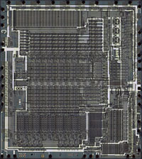
SID / MOS 6581 R2
.jpg)
MOS 6581 R2 Overview low quality (JPG, 15 MB)
MOS 6581 R2 Overview medium quality (JPG, 21 MB)
MOS 6581 R2 Overview high quality (JPG, 39 MB)
MOS 6581 R2 Overview stitched TIFF 400 MB
MOS 6581 R2 raw images in xxyy.png naming.
further images and analysis at Tommis site
Revectorized die by Tommi
R2 vs R3 comparison by Tommi
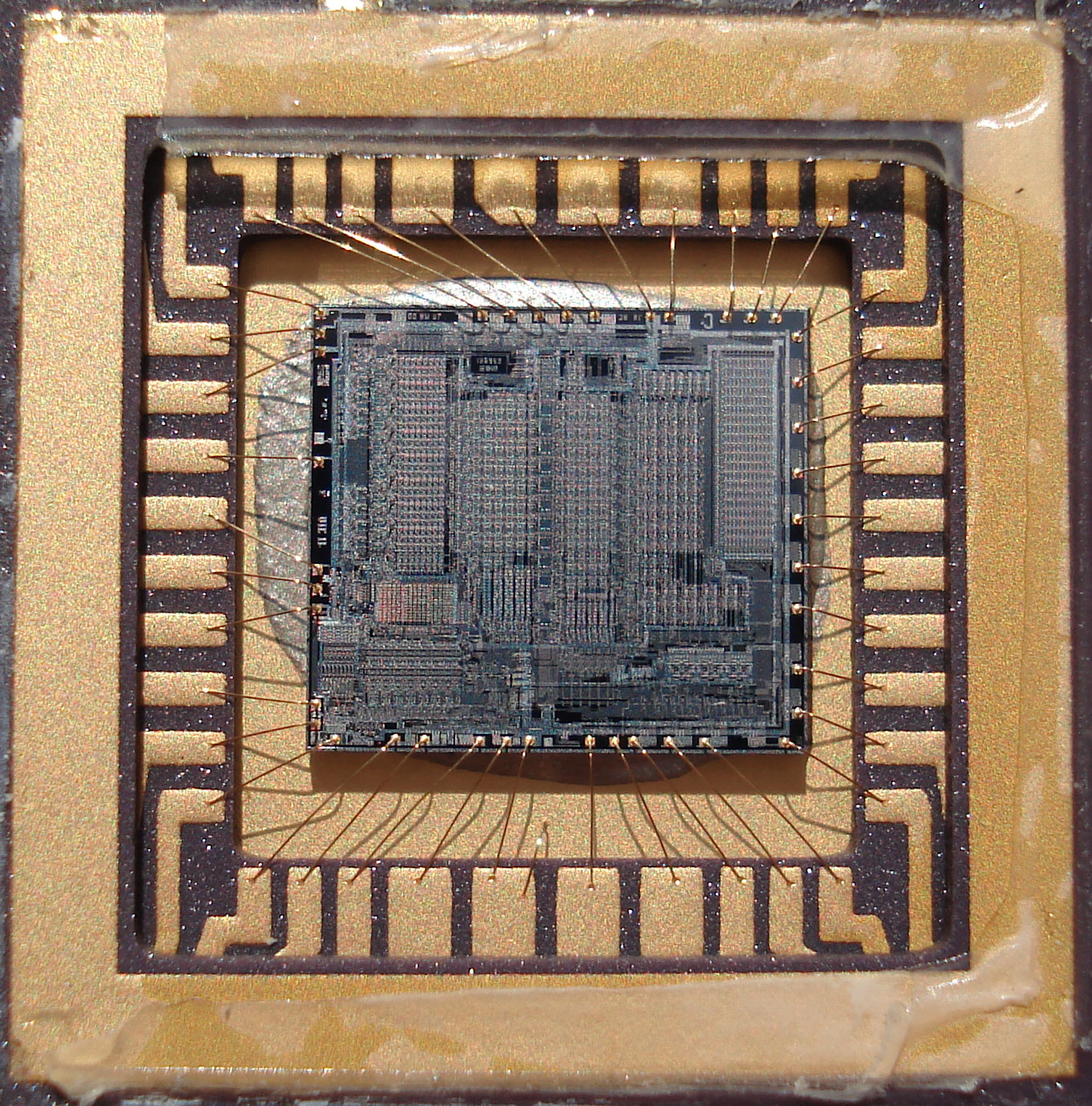
SID / MOS 6581 R3
A typical SID 6581 R3. Shown here is the chip that was measured for the 'enigma R3 4885' filter curve used in various emulators and sid players.
I got this chip from Tommi Lempinen aka ZeroX. Defect unknown (was it defect before opening?).
The package opening process was described by Tommi: "Anywho, the process I took to open it was to heat up the stove to the max, then left the chip on it (damn what horrible smell it was). After a bit of smoke I dropped the chip into cold water, then repeated the heating and cooling. Finally took two pliers and cracked open the package, and there was the die."
MOS 6581 R3 Overview (JPG, 50 MB)
MOS 6581 R3 Overview stitched TIFF 430 MB
MOS 6581 R3 additional content incl. filter, cut-off msb, volume control, resonance control, output stage in darkfield mode
MOS 6581 R3 raw images in xxyy.png naming. Including filter and darkfield subfolders. Stepwidth in X 0.5 mm, Y 0.42 mm.
further images and analysis at Tommis site
Revectorized die by Tommi
The analog filter circuity seem to have two similar parts. So I imaged the left part in higher resolution. Focus plane is on the brown layer. This seems to be the limit a normal visible light microscope is capable of. This area is near the lower right edge of the die.
SID 6581 R3 left half of analog filter at very high magnification 1/2 resolution, JPEG quality 15%. This was stitched from about 20 images.
Additional 3 images of the same area with focus plane on the topmost metal layer (JPEG Quality 15%):
SID 6581 R3 detailed analog filter 1
SID 6581 R3 detailed analog filter 2
SID 6581 R3 detailed analog filter 3
Detailed images taken at a higher resolution and the same area with different focus planes:
Least significant bit of Volume control 1
Least significant bit of Volume control 2
least or most significant bit of resonance control 1
least or most significant bit of resonance control 2
ext-in-to-filter control bit 1
ext-in-to-filter control bit 2
most significant bit of cutoff ? 1
most significant bit of cutoff ? 2
Darkfield images:
SID 6581 R3 output stage, 100% resolution, 30% JPEG quality.
SID 6581 R3 audio amplifier, 100% resolution, 60% JPEG quality.
SID 6581 R3 filter stage, 100% resolution, 60% JPEG quality.
SID 6581 R3 lookup table?, 100% resolution, 60% JPEG quality.
SID 6581 R3 something else?, 100% resolution, 60% JPEG quality.
SID / MOS 6581 R4
.jpg)
I got the chip from Jarkko Lehti aka Grue / Beyond Force. It has the date code week 34 1988. Some comparison checks with a CSG 6581 week 37 1989 indicate that the dies are identical. The second SID was also from Grue. The die seems to be nearly identical to the R3, especially in the filter area. Noticeable are the color differences of the oxide layer. The differences are real since the microscope light source is calibrated to 3200K color temperature. The guess is that the different behaviour of the filter relates to some material change. The different properties could be checked with spectroscopic methods on the micrometer scale, e.g. EDX (Energy-dispersive X-ray spectroscopy).
MOS 6581 R4 Overview (JPG low quality, 30 MB)
MOS 6581 R4 analog filter (JPG low quality)
MOS 6581 R4 Logo in high magnification (JPG low quality)
MOS 6581 R4 filter related circuit (JPG low quality)
MOS 6581 R4 filter related circuit (JPG low quality)
MOS 6581 R4 Overview (JPG, 50 MB)
MOS 6581 R4 Logo TIFF
MOS 6581 R4 Overview (TIFF, 1 GB)
MOS 6581 R4 raw images in xxyy.png naming.
further images and analysis at Tommis site
Revectorized die by Tommi
Comparison images of the second SID CSG 6581 R4AR 3789.
SID / MOS 8580 R5
.jpg)
I got the chip from Jarkko Lehti aka Grue / Beyond Force. It has the date code week 02 1988. Some comparison checks with a CSG 8580 week 05 1991 indicate that the dies are identical.
MOS 8580 R5 Overview (JPG low quality, 24 MB)
MOS 8580 R5 Overview (JPG, 42 MB)
MOS 8580 R5 Overview (TIFF, 390 MB)
MOS 8580 R5 Overview (TIFF with layers, 790 MB)
MOS 8580 R5 raw images in xxyy.png naming.
further images and analysis at Tommis site
Revectorized die by Tommi
REU Controller / MOS 8726 R1
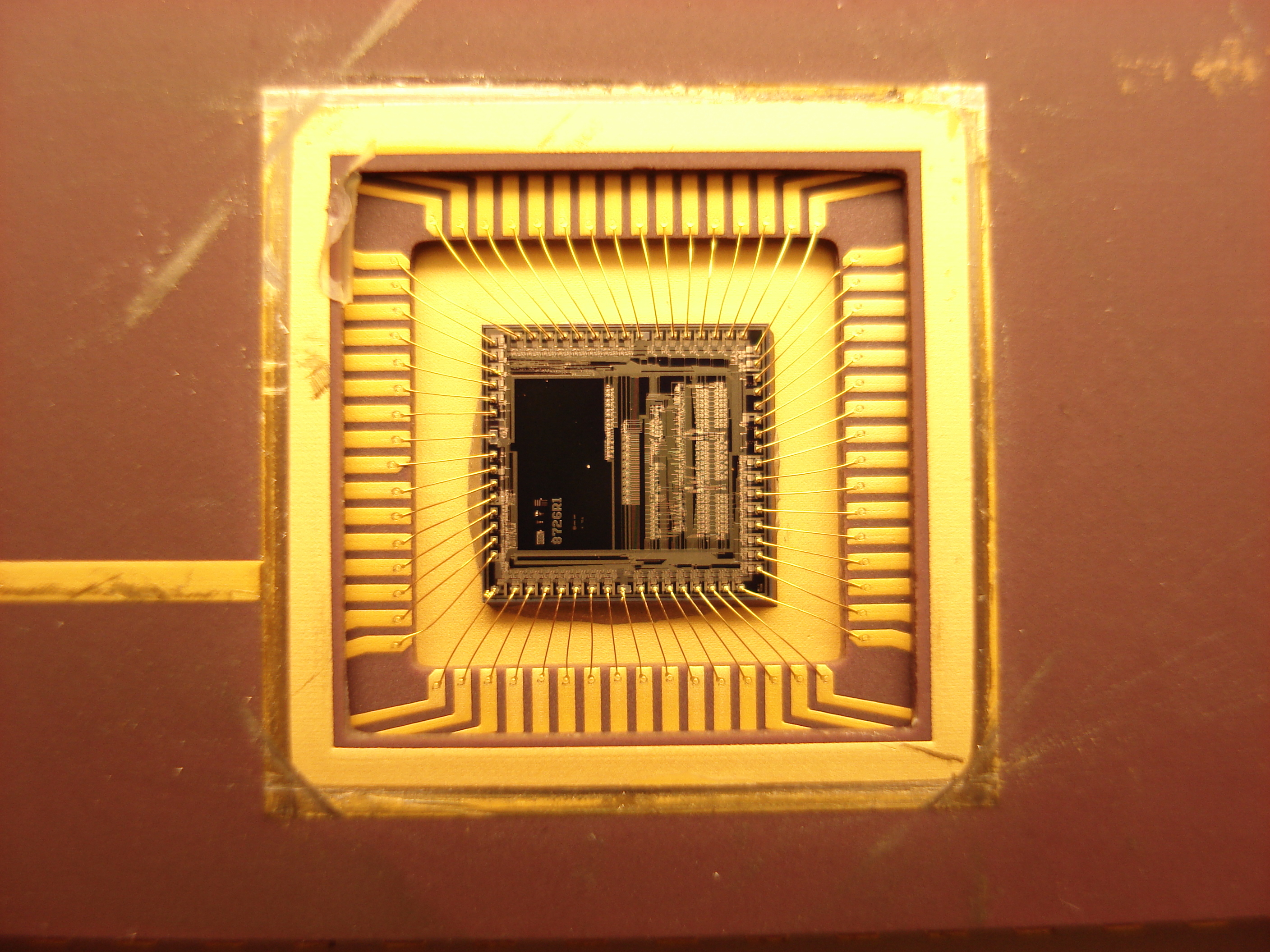
MOS 8726 R1 Overview (JPG low quality, 20 MB)
MOS 8726 R1 Overview (JPG, 49 MB)
MOS 8726 R1 Overview (TIFF, 503 MB)
MOS 8726 R1 Overview (TIFF layers, 1.3 GB)
MOS 8726 R1 raw images in xx_yy.png naming.
Links
All chip images on ftpTommis Lempinens site who put a tremendeous effort in reworking and collaborative analysing the chips.
Visual 6502.org
Kevtris Blog with articles and insights of CBM chips.
Jim Butterflys site with tech docs of the C64.
MOS 8500R4
